INTERACT FORUM

Please login or register.

Login with username, password and session length
Advanced search  
Pages: [1]   Go Down

Author Topic: What is 22nm technology?  (Read 12179 times)

JimH

  • Administrator
  • Citizen of the Universe
  • *****
  • Posts: 71660
  • Where did I put my teeth?
What is 22nm technology?
« on: May 12, 2012, 06:46:34 pm »

Intel uses 22nm technology in making the new Ivy Bridge CPU's.  I've been trying to understand what it's all about.  Here's my source:

http://en.wikipedia.org/wiki/22nm

The 22nm is an index of the distance between discrete elements of the die.  I think so at least.

I say index because its a measure of how far each transistor is set back from the centerline.  Any two elements are actually 44nm apart.

A nanometer is a billionth of a meter.  It's ten angstroms.

For comparison, a Ribosome, which I think is a strand of DNA, is about 20nm.

I've read that Intel intends to step down a couple times more to 10nm technology by about 2016.

This is hard to grasp.
Logged

Scolex

  • MC Beta Team
  • Citizen of the Universe
  • *****
  • Posts: 1116
  • Cheers
Re: What is 22nm technology?
« Reply #1 on: May 12, 2012, 06:54:01 pm »

Very hard to grasp when you consider that a hair is about 100,000 nanometers in diameter.
Logged
Sean

hulkss

  • Galactic Citizen
  • ****
  • Posts: 447
Re: What is 22nm technology?
« Reply #2 on: May 12, 2012, 11:04:31 pm »

This is the best explanation of size that I have ever seen :o

http://uploads.ungrounded.net/525000/525347_scale_of_universe_ng.swf

Logged

MrC

  • Citizen of the Universe
  • *****
  • Posts: 10462
  • Your life is short. Give me your money.
Re: What is 22nm technology?
« Reply #3 on: May 12, 2012, 11:09:52 pm »

Update to V2.0!

  http://htwins.net/scale2/
Logged
The opinions I express represent my own folly.

hulkss

  • Galactic Citizen
  • ****
  • Posts: 447
Re: What is 22nm technology?
« Reply #4 on: May 12, 2012, 11:11:42 pm »

Thanks for the update.

Here's another (bigger I guess) http://htwins.net/scale2/scale2.swf?bordercolor=white
Logged

Audioseduction

  • World Citizen
  • ***
  • Posts: 125
  • World Class Referance Playback!
Re: What is 22nm technology?
« Reply #5 on: May 14, 2012, 09:53:51 am »

They must have retrieved the technology from a crashed UFO.  ;D
Logged

KingSparta

  • MC Beta Team
  • Citizen of the Universe
  • *****
  • Posts: 20054
Re: What is 22nm technology?
« Reply #6 on: May 14, 2012, 07:57:36 pm »

I have a vacuum tube radio, It still works.

It's amazing where technology started, and where it is today.
Logged
Retired Military, Airborne, Air Assault, And Flight Wings.
Model Trains, Internet, Ham Radio
https://MyAAGrapevines.com
https://centercitybbs.com
Fayetteville, NC, USA

InflatableMouse

  • MC Beta Team
  • Citizen of the Universe
  • *****
  • Posts: 3978
Re: What is 22nm technology?
« Reply #7 on: May 15, 2012, 02:02:22 pm »

I'm trying to find the quote from one of Intel's big engineers when he said they had reached the limits of what was possible. It just can't get any smaller than this, he said. I think that was during the release of the first Pentium processor. I wonder if he still works there ;).
Logged

KingSparta

  • MC Beta Team
  • Citizen of the Universe
  • *****
  • Posts: 20054
Re: What is 22nm technology?
« Reply #8 on: May 15, 2012, 07:14:24 pm »

I think the same was said about storage on hard drives.
Logged
Retired Military, Airborne, Air Assault, And Flight Wings.
Model Trains, Internet, Ham Radio
https://MyAAGrapevines.com
https://centercitybbs.com
Fayetteville, NC, USA

Matt

  • Administrator
  • Citizen of the Universe
  • *****
  • Posts: 42049
  • Shoes gone again!
Logged
Matt Ashland, JRiver Media Center

newsposter

  • MC Beta Team
  • Citizen of the Universe
  • *****
  • Posts: 787
Re: What is 22nm technology?
« Reply #10 on: May 17, 2012, 04:20:59 pm »

IBM already has 5nm working and has demo-ed their PPC and mainframe CPU 'books' fabbed in 5nm.
Logged

glynor

  • MC Beta Team
  • Citizen of the Universe
  • *****
  • Posts: 19608
Re: What is 22nm technology?
« Reply #11 on: May 17, 2012, 05:25:27 pm »

The 22nm is an index of the distance between discrete elements of the die.  I think so at least.

Not quite.

The reported "size" at a particular process node (22nm in this case) is the average half-pitch of a single DRAM cell (that's simplifying somewhat, but it works for this discussion).  The pitch is often reported to be the "distance between cells".  That's not entirely accurate, the way most people think about it, because it assumes that the "cells" themselves take up no space at all.  That's not what it means.

The DRAM half-pitch is roughly the size of the average DRAM cell at a particular process node.  Despite the fact that they are "manufactured", the cell size does vary from transistor to transistor.  Measuring actual transistors isn't easy.  Because they are three-dimensional (and infinitesimally small) is difficult tell where the transistor itself begins and ends.  However, you can accurately measure the distance across the cells, using the contacts as your "border".  One-half of that distance, roughly correlates to the size of the transistor within.  Pictures make it clear:


If you look at any modern CPU core under a microscope, you can see that the DRAM cache actually takes up a substantial amount of the surface area of the chip:


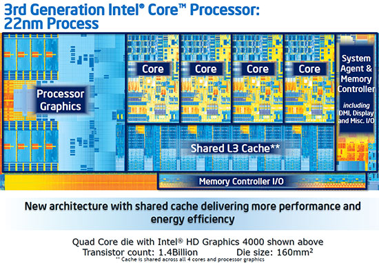
See all the "boring-blue" sections in each of the different cores?  That's all memory cells, as is the entire L3 cache area.

Plus, because memory cells are fundamental and relatively simple, that's typically the first thing at any process node that they push out (those ultra-tiny "demos" that IBM and others have shown are all made up of sometimes-functional-sometimes-not DRAM cells, or NAND which is even easier to get down to very small feature sizes).  And, different functional units are actually shaped/sized differently, so you can't just say a blanket "our transistors are x size" across an entire complex chip.

So, at any given process node, the "size" given is more of an average feature size.  Specifically, it correlates to the DRAM cell size, which is usually the most common transistor on any given chip, but even if not, the lithography process is all the same size, so they other features' sizes correlate to the DRAM cell size.

Make sense?
Logged
"Some cultures are defined by their relationship to cheese."

Visit me on the Interweb Thingie: http://glynor.com/

glynor

  • MC Beta Team
  • Citizen of the Universe
  • *****
  • Posts: 19608
Re: What is 22nm technology?
« Reply #12 on: May 17, 2012, 05:35:41 pm »

PS. If you are a huge nerd and you want to know more, it would be best to go to the source reports:

http://www.itrs.net/Links/2011ITRS/Home2011.htm
Logged
"Some cultures are defined by their relationship to cheese."

Visit me on the Interweb Thingie: http://glynor.com/

chidino

  • Member
  • *
  • Posts: 1
Re: What is 22nm technology?
« Reply #13 on: May 17, 2012, 11:29:20 pm »

And on the storage front:

http://en.wikipedia.org/wiki/Heat-assisted_magnetic_recording

"Seagate believes it can produce 300 terabit (37.5 terabyte) Hard disk drives using HAMR technology."  That's in a 3.5" drive.  Supposedly, they're talking 2014-2015.
Logged

Sparks67

  • World Citizen
  • ***
  • Posts: 162
Re: What is 22nm technology?
« Reply #14 on: July 22, 2012, 12:20:51 pm »

PS. If you are a huge nerd and you want to know more, it would be best to go to the source reports:

http://www.itrs.net/Links/2011ITRS/Home2011.htm

No, if you are a real huge nerd, and want to follow the technology as it develops then you need to follow the paper level.  So, this http://www.itrs.net/links.html shows you the links, but one is IEEE. 
or SPIE is the easy ones.   Now to read the academic papers, then you need access to them.  Most of your local universities will have access to these journals, so you can follow the technology easier.   You can also join IEEE or SPIE, but usually the cost is $135 a year to join.  There is conferences that you might like to attend, and usually it varies in a rather nice place to visit.  Sometimes your job might pay for these memberships, and you can attend these conferences. 

Logged

Sparks67

  • World Citizen
  • ***
  • Posts: 162
Re: What is 22nm technology?
« Reply #15 on: July 22, 2012, 12:58:55 pm »

And on the storage front:

http://en.wikipedia.org/wiki/Heat-assisted_magnetic_recording

"Seagate believes it can produce 300 terabit (37.5 terabyte) Hard disk drives using HAMR technology."  That's in a 3.5" drive.  Supposedly, they're talking 2014-2015.

HAMR been in development since I think 2006, but perhaps earlier.  Seagate will probably have a 5 to 6 Terabyte disc in 2015, and then the plans is by 2019.  Seagate plans up to 60 Terabyte disc. 
It is one of the key technologies for UHDTV, and you will see Holographic storage as the other technology.  Most people don't understand that to develop UHDTV, there is several technologies that are being developed.  One is how to store these massive files for 4k and 8k video.  Anyway, here is a an easy to read paper from NHK on it.   There are several companies besides Seagate that are developing their own format. 

http://www.nhk.or.jp/strl/publica/bt/en/ch0040.pdf

I am personally more interested in Holographic storage, because you need a way to backup your data or videos etc.  As you expand beyond several terabytes, then there is really no cheap solution.  I prefer an optical format solution.  Here is a blog from Hitachi Data Systems, they are one the key developers.  http://blogs.hds.com/technomusings/2011/08/a-true-holographic-system-would-be-disruptive.html
InPhase Technology went bankrupt in 2010, but they have reappeared in 2012 basically under a new name.  That is hVault, but some of the key people that worked at InPhase Technology are now at hVault. 

Ok, I am off topic again...


Logged
Pages: [1]   Go Up